|
|
8 years ago | |
|---|---|---|
| box | 8 years ago | |
| doc | 8 years ago | |
| footprints | 8 years ago | |
| pic | 8 years ago | |
| plot | 8 years ago | |
| spice | 9 years ago | |
| tools | 9 years ago | |
| .gitignore | 9 years ago | |
| README.md | 8 years ago | |
| analog.bak | 8 years ago | |
| analog.sch | 8 years ago | |
| blinkey.bak | 8 years ago | |
| blinkey.sch | 8 years ago | |
| flash.bak | 8 years ago | |
| flash.sch | 8 years ago | |
| fp-lib-table | 8 years ago | |
| gpdi.bak | 8 years ago | |
| gpdi.sch | 8 years ago | |
| gpio.bak | 8 years ago | |
| gpio.sch | 8 years ago | |
| power.bak | 8 years ago | |
| power.sch | 8 years ago | |
| ram.bak | 8 years ago | |
| ram.sch | 8 years ago | |
| sdcard.bak | 8 years ago | |
| sdcard.sch | 8 years ago | |
| ulx3s-cache.lib | 8 years ago | |
| ulx3s-rescue.lib | 8 years ago | |
| ulx3s.bak | 8 years ago | |
| ulx3s.kicad_pcb | 8 years ago | |
| ulx3s.kicad_pcb-bak | 8 years ago | |
| ulx3s.pro | 8 years ago | |
| ulx3s.sch | 8 years ago | |
| usb.bak | 8 years ago | |
| usb.sch | 8 years ago | |
| wifi.bak | 8 years ago | |
| wifi.sch | 8 years ago | |
README.md
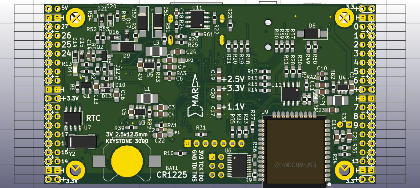
ULX3S PCB
This is work-in-progress place for putting some wishes of a small (94x51 mm) FPGA board.
ULX3S = University digital logic Learning eXtensible board release 3 with SDRAM, Successor of ULX2S.
kicad ulx3s.pro
Schematics is mostly complete. PCB v1.7 is produced and big things work like USB-JTAG, SDRAM, SDCARD, HDMI, FLASH, RTC, I2C, OLED, AUDIO, ADC but there are issues, luckily most can be fixed by Upgrading PCB v1.7. USB2 and 433.92MHz antenna are currently untested.
3D preview
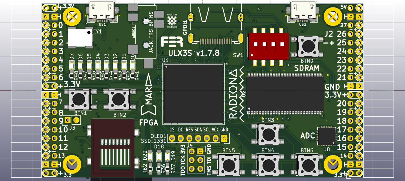
Features
FPGA: Lattice ECP5 LFE5U-45F-6BG381C
USB: FTDI FT231XS (300kbit JTAG and 3Mbit USB-serial)
GPIO: 56 pins (28 differential pairs), PMOD-friendly
RAM: 32MB SDRAM MT48LC16M16
Flash: 4MB SPI Flash IS25LP032D for FPGA config
Storage: Micro-SD slot
LEDs: 11 (8 blink-LEDs, 2 USB LEDs, 1 WiFi LED)
Buttons: 7 (4 direction, 2 fire, 1 power button)
Audio: 3.5 mm jack with 4 contacts (analog stereo + digital audio or composite video)
Video: GPDI connector with 3.3V-5V I2C bidirectional level shifter
Display: placeholder for 0.96" SPI COLOR OLED
WiFi+bluetooth: placeholder for ESP-32 (Standalone JTAG web interface over WiFi)
ADC: 8 channels, 8 bit, 1 MSa/s MAX11123
Power: 3 Switching voltage regulators: 1.1V, 2.5V, 3.3V
Clock: 25 MHz onboard, external differential clock input
Low power sleep: RTC clock wakeup, power button, 32768 Hz quartz and battery
GPDI is General Purpose Differential Interface, Electrically LVDS, mostly TMDS tolerant female receptacle more-or-less compatible with digital monitors/TVs
Todo
Test the prototype.
[x] Silkscreen Double outline for BGA chip
[x] Silkscreen do not write over the solder pads
[ ] Silkscreen BGA names on ESP32 placeholder and 2.54 mm headers
[x] Silkscreen JTAG signal names on 6-pin 2.54 mm header
[x] Silkscreen remove OLED outline
[x] Solder stop mask must go inbetween all SMD chip pads
[x] External differential clock input at J1_33 +/-
[x] physically sprinkle VCC blocator capacitors under BGA
[ ] Values on silkscreen
[x] Dedicated antenna pin
[x] onboard 433 antenna
[x] 433 remove GND and silkscreen test point
[x] Resistors for LEDs
[x] Move USB LEDs from bottom to top side
[x] Improve SDRAM routing - use VIAs for closest pins
[x] Increase thickness of power lines (5V, 3.3V, 2.5V)
[x] Compile a f32c bitstream using the schematics
[x] Compile differential GPDI output
[x] Connect more lines from ESP-32 to FPGA
[x] Connect FPGA USB D+/D- with 1.5k pullup in USB 1.1 (full speed) mode
[x] FPGA USB add 27 ohm + 3.6 V zener
[x] Symmetrically place USB connectors left-right
[ ] Jumpers to switch 2.5V/3.3V for left IO banks
[x] External JTAG header
[x] Move JTAG 2 mm left
[x] Move WiFi Disable jumper closer to the BTN1 (angled header)
[x] Sprinkle 2.2uF capacitors on power lines
[x] Spice simulation of power-up/shutdown network
[x] 27ohm D+/D- to FT231XS
[x] DIP switch (4 switches)
[x] MAX11123 ADC SPI
[x] I2C for RTC
[x] main usb connector on top side
[x] space screw to other parts
[x] move battery away from screw hole
[x] top layer GND fill
[x] R25 move away from oled screw hole
[ ] board cut off notches inisde for space saving
[x] DIP switch to the right near RAM
[x] Move HDMI a bit closer to OLED
[x] 32768Hz oscillator footprint
[x] SD card footprint SCHD3A0100
[x] center the SD footprint for T&R
[x] SD connect GND (thin pins)
[x] move USB 0.5-1mm more out
[x] DIP SW footprint correct
[x] AUDIO jack footprint fits
[x] AUDIO jack pin 4 (ring2) connected to 4-bit DAC
[x] BTN footprint too small
[x] SMPS jumpers default OFF for prototype testing
[x] FPGA DONE to ESP-32
[x] Diodes manual soldering
[x] R56: FT231X rev A,B,C TXDEN to GND
    workaround from TN140_FT231X Errata
[x] PCB for LFE5UM ready (some GND will change to
    VCC for Serdes power supply, see LFE5U->LFE5UM
    migration docs)
[x] Check GND/VCC for 45 and 85 packages,
    for example pin T11 is NC on 25U, GND on 85U and VCC ond 85UM
[x] Reconnect WIFI_OFF so that jumper has priority
[x] 25MHz oscillator: needs clearance from LEDs, move under USB1
[x] connect SHUTDOWN to FPGA
[ ] ESP-32: GPIO12 at boot selects internal flash voltage,
    it is connected to J1_27+ and wrong pullup/pulldown at boot
    will prevent ESP32 from booting
[x] ESP-32: won't boot when SD connected. Don't solder it at PCB v1.7
    it should be routed differently in newer release
    Here is a possible SD card connection
    Arduino->Examples->ESP32->SD_MMC_Test
    https://github.com/espressif/esp-idf/blob/master/examples/storage/sd_card/README.md
    move blue LED from GPIO2 to GPIO17
[ ] SD card pullup pulldowns (do we need them if FPGA can pullup/pulldown)
[x] I2C resistors increased 470->2.2k
[ ] GPDI series C=100nF to each differential line.
[x] reliable shutdown (D11=RED LED, R4=4.7k)
[x] SDRAM raster back to 0.8 mm
[x] connect SPI Flash Quad Mode (QSPI)
[x] allow powering the board without powering FTDI chip
[ ] reverse D9 at US2 to draw power from usb instead of provide it
[x] micro USB extended pads for Handsoldering (already were extended)
[x] move 25MHz oscillator away from USB connector for handsoldering
[x] schematics gpio J..+- pins renamed to gp/gn for easier readability
[ ] Make BOM outputtable from PCB->Files->Fabrication Outputs->BOM file
[ ] route 16-channel ADC
[x] move 8 LEDs a bit down and right