|
|
8 years ago | |
|---|---|---|
| box | 8 years ago | |
| doc | 8 years ago | |
| footprints | 8 years ago | |
| home | 8 years ago | |
| pic | 8 years ago | |
| plot | 8 years ago | |
| spice | 8 years ago | |
| tools | 8 years ago | |
| .gitignore | 9 years ago | |
| 1-click-bom.tsv | 8 years ago | |
| README.md | 8 years ago | |
| analog.bak | 8 years ago | |
| analog.sch | 8 years ago | |
| blinkey.bak | 8 years ago | |
| blinkey.sch | 8 years ago | |
| bom.ini | 8 years ago | |
| flash.bak | 8 years ago | |
| flash.sch | 8 years ago | |
| fp-lib-table | 8 years ago | |
| gpdi.bak | 8 years ago | |
| gpdi.sch | 8 years ago | |
| gpio.bak | 8 years ago | |
| gpio.sch | 8 years ago | |
| kitspace.yaml | 8 years ago | |
| power.bak | 8 years ago | |
| power.sch | 8 years ago | |
| ram.bak | 8 years ago | |
| ram.sch | 8 years ago | |
| sdcard.bak | 8 years ago | |
| sdcard.sch | 8 years ago | |
| sym-lib-table | 8 years ago | |
| ulx3s-cache.lib | 8 years ago | |
| ulx3s-rescue.lib | 8 years ago | |
| ulx3s.bak | 8 years ago | |
| ulx3s.kicad_pcb | 8 years ago | |
| ulx3s.kicad_pcb-bak | 8 years ago | |
| ulx3s.pro | 8 years ago | |
| ulx3s.sch | 8 years ago | |
| usb.bak | 8 years ago | |
| usb.sch | 8 years ago | |
| wifi.bak | 8 years ago | |
| wifi.sch | 8 years ago | |
README.md
ULX3S PCB
ULX3S = University digital Logic Learning Xtensible board release 3 with SDRAM, Successor of ULX2S.
3D preview
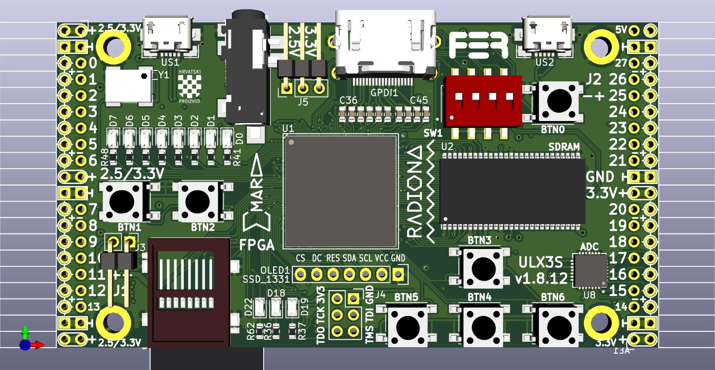
This is a small (94x51 mm) standalone FPGA board for education, research and general purpose, with a full featured selection of chips which I all wanted on a low-cost PCB, but haven't found on the market. It's open source and open hardware because if it is good for our development of f32c SOC, it should be also good to other projects.
ULX3S will carry all digital logic on our research, education and makerspace projects in next 5 years.
ULX3S is standalone embeddable gadget with onboard display, buttons, storage, WiFi and compatible connectors.
ULX3S can do things no other board can.
ULX3S can self-reflash with a bitstream sent remotely from web interface over WiFi or from SD card browsed by onboard OLED display and buttons.
ULX3S can completely power down and wakeup from battery backed RTC.
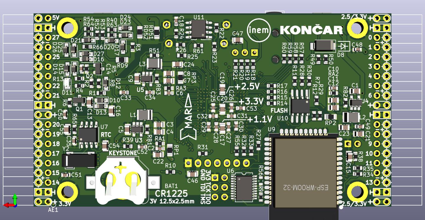
ULX3S has rich range of chips and connectivity required for many other open source projects: SDRAM, USB, PS/2, SDCARD, HDMI, FLASH, RTC, I2C, OLED, AUDIO, ADC, onboard FM/ASK antenna 88-433.92 MHz and 56 GPIO pins which are all routed as differential pairs and have pinout that is PMOD compatible.
ULX3S is sufficiently equipped to emulate Amiga retro computer and run its games, but can do much more.
Schematics and PCB started with KiCAD 4. After version v1.8 project switched to KiCAD 5 PCB editor:
kicad ulx3s.pro
Features
FPGA: Lattice ECP5 LFE5U-85F-6BG381C (85K LUT)
USB: FTDI FT231XS (300kbit JTAG and 3Mbit USB-serial)
GPIO: 56 pins (28 differential pairs), PMOD-friendly
RAM: 32MB SDRAM MT48LC16M16
Flash: 4MB Quad-SPI Flash IS25LP032D for FPGA config
Storage: Micro-SD slot
LEDs: 11 (8 blink-LEDs, 2 USB LEDs, 1 WiFi LED)
Buttons: 7 (4 direction, 2 fire, 1 power button)
Audio: 3.5 mm jack with 4 contacts (analog stereo + digital audio or composite video)
Video: GPDI connector with 3.3V-5V I2C bidirectional level shifter
Display: placeholder for 0.96" SPI COLOR OLED
WiFi+bluetooth: placeholder for ESP-32 (Standalone JTAG web interface over WiFi)
ADC: 8 channels, 12 bit, 1 MSa/s MAX11125
Power: 3 Switching voltage regulators: 1.1V, 2.5V, 3.3V
Clock: 25 MHz onboard, external differential clock input
Low power sleep: RTC clock wakeup, power button, 32768 Hz quartz and battery
GPDI is General Purpose Differential Interface, Electrically LVDS, mostly TMDS tolerant female receptacle more-or-less compatible with digital monitors/TVs
Production
ZIP the gerbers and send them to manufacturer:
zip -r /tmp/ulx3s.zip plot/ulx3s
If you are going to order this project by yourself, it is important what manufacturer to choose for PCBA (PCB and Assembly) service.
Choose PCBA manufacturer which can produce PCB of IPC CLASS 3 quality, 5/5 mil trace resolution and 0.2 mm holes. Avoid manufacturer who claims "quality" and "satisfaction" but doesn't really know what will be IPC CLASS rating for this project.
PCBA manufacturer prices for the parts should be approximately equal as those from distributors like Mouser or DigiKey. Avoid any PCBA manufacturer who asks 3$ for the 1$ part or 40$ for the 30$ part. Select Mouser language/location icon to PCBA manufacturer country of origin and $-currency to check is PCBA manufacturer telling the truth about prices.
Before soldering the parts, ask manufacturer for pictures of PCB. CLASS 3 demands, among other things, that all drill holes stay inside of VIA pads. If some holes break-out from pads, ask manufacturer to make new PCBs with better drill and copper layer alignment.
PCBCART offers CLASS 3 quality and assembly at reasonable cost. Prices for the parts are equal to Mouser.
Don't pay everything at once. Following payment phases during the PCBA production are recommended:
1. Pay for the parts
2. Manufacturer orders the parts and optionally negotiates with you about part numbers.
   Depending on market availability, some parts may come in different physical package.
3. Send updated gerbers which fit to ordered parts.
4. Pay for PCB
5. Manufacturer sends pictures of produced PCB for your inspection.
   If anything looks suspicious, ask also for X-ray imaging.
6. Pay for the assembly and shipping.
Nobody wants quality issues, so it is good to ask if manufacturer has qualified personnel able to follow instructions for ULX3S self-test before shipping.
Todo
Here is checklist what was done or should be done in the next PCB release.
[x] Silkscreen Double outline for BGA chip
[x] Silkscreen do not write over the solder pads
[x] Silkscreen JTAG signal names on 6-pin 2.54 mm header
[x] Silkscreen remove OLED outline
[x] Solder stop mask must go inbetween all SMD chip pads
[x] External differential clock input at J1_33 +/-
[x] physically sprinkle VCC blocator capacitors under BGA
[ ] Values on silkscreen
[x] Dedicated antenna pin
[x] onboard 433 antenna
[x] 433 remove GND and silkscreen test point
[x] Resistors for LEDs
[x] Move USB LEDs from bottom to top side
[x] Improve SDRAM routing - use VIAs for closest pins
[x] Increase thickness of power lines (5V, 3.3V, 2.5V)
[x] Compile a f32c bitstream using the schematics
[x] Compile differential GPDI output
[x] Connect more lines from ESP-32 to FPGA
[x] Connect FPGA USB D+/D- with 1.5k pullup in USB 1.1 (full speed) mode
[x] FPGA USB add 27 ohm + 3.6 V zener
[x] Symmetrically place USB connectors left-right
[x] External JTAG header
[x] Move JTAG 2 mm left
[x] Move WiFi Disable jumper closer to the BTN1 (angled header)
[x] Sprinkle 2.2uF capacitors on power lines
[x] Spice simulation of power-up/shutdown network
[x] 27ohm D+/D- to FT231XS
[x] DIP switch (4 switches)
[x] MAX11123 ADC SPI
[x] I2C for RTC
[x] main usb connector on top side
[x] space screw to other parts
[x] move battery away from screw hole
[x] top layer GND fill
[x] R25 move away from oled screw hole
[x] DIP switch to the right near RAM
[x] Move HDMI a bit closer to OLED
[x] 32768Hz oscillator footprint
[x] SD card footprint SCHD3A0100
[x] center the SD footprint for T&R
[x] SD connect GND (thin pins)
[x] move USB 0.5-1mm more out
[x] DIP SW footprint correct
[x] AUDIO jack footprint fits
[x] AUDIO jack pin 4 (ring2) connected to 4-bit DAC
[x] BTN footprint too small
[x] SMPS jumpers default OFF for prototype testing
[x] FPGA DONE to ESP-32
[x] Diodes manual soldering
[x] R56: FT231X rev A,B,C TXDEN to GND
    workaround from TN140_FT231X Errata
[x] PCB for LFE5UM ready (some GND will change to
    VCC for Serdes power supply, see LFE5U->LFE5UM
    migration docs)
[x] Check GND/VCC for 45 and 85 packages,
    for example pin T11 is NC on 25U, GND on 85U and VCC ond 85UM
[x] Reconnect WIFI_OFF so that jumper has priority
[x] 25MHz oscillator: needs clearance from LEDs, move under USB1
[x] connect SHUTDOWN to FPGA
[x] ESP-32: won't boot when SD connected. Don't solder it at PCB v1.7
    It is routed differently in newer release
    Arduino->Examples->ESP32->SD_MMC_Test
    https://github.com/espressif/esp-idf/blob/master/examples/storage/sd_card/README.md
    moved blue LED from GPIO2 to GPIO5
[x] I2C resistors increased 470->2.2k
[x] GPDI AC-coupling 100nF to each differential line.
[x] reliable shutdown (D11=RED LED, R4=4.7k)
[x] SDRAM raster back to 0.8 mm
[x] connect SPI Flash Quad Mode (QSPI)
[x] allow powering the board without powering FTDI chip
[ ] reverse D9 at US2 to draw power from usb instead of provide it
[x] micro USB extended pads for Handsoldering (already were extended)
[x] move 25MHz oscillator away from USB connector for handsoldering
[x] schematics gpio J..+- pins renamed to gp/gn for easier readability
[ ] route 16-channel ADC
[x] move 8 LEDs a bit down and right
[x] let SD_CLK go to FPGA clock capable pin: swap SD_CLK and SD_D2 pins
[x] additional 2 differential lines for US2
[x] additional US2 pins for pullup 1.5k
[x] additional US2 pins for pull up-down 15k
[x] unified US2 pullup/down: resistor-diode nework for pullup 1.5k and pulldown 15k
[x] clear silkscreen mess with Cx under FPGA
[x] power decoupling capacitors for ESP32 and OLED
[x] Connect switching power supply jumpers
[ ] every 1-2 seconds there are clicks at analog audio output
[x] 3.6V zener diodes must be on FPGA side
[x] can esp32 second tx/rx port make serial communication with FPGA
[x] Jumper to switch 2.5V/3.3V for left IO banks
[x] move usb pull from gpio bank0 to gpdi bank1
[x] isolate each PMOD group to each io bank
[ ] move GP7,GP8 from gpio bank0 to gpio bank7
[x] route selected voltage to VCCio0/7
[x] route selected voltage to J1 PMOD instead of 3.3V fixed
[x] more bank0,1,7 decoupling capacitors
[x] Move Jumper 2.5V/3.3V deeper inside PCB (angled header)
[x] 0R resistor placeholders to hardwire 2.5V/3.3V instead of the jumper
[x] Selected 2.5/3.3V to J1 header (instead fixed 3.3V)
[x] RTC battery capacitor
[x] battery + pad clearance
[x] PCB v1.8.1 redesigned to fit HDMI 649-10029449-111RLF (the cheapest)
[ ] use cheaper diodes 583-MM4148-T in SOD-80C package
[x] fix copper layer after using non-handsoldering resistor footprints
[x] DIP switch must be pulled up at 2.5/3.3V or 2.5V line, not 3.3V
[x] RTC time loss at power down fixed with 1k+22uF - see page 54 of datasheet
[x] Rotate SD card 180° for easier front loading
[x] Move C1, C21, C50 away from J1, J2 connectors (make space for IDC header)
[x] Smaller USB pads
[x] Smaller pads (not for handsoldering)
[x] Revert USB to datasheet default
[x] ADC text smaller font, move above ADC chip
[x] ULX3S/version left of ADC chip
[x] (inem) KONCAR logo on bottom side
[x] BTN font size like TCK
[x] Combo pads for flash 150/208 mil
[x] SDRAM text smaller font size
[x] SW1 increase size, to more visible place
[x] GPIO numbering on bottom side, all pins in smaller font
[x] enlarge FER logo
[x] Descriptive audio jack schematic symbol
[x] USB ID pin to RTC WAKEUPn
[ ] Move 25MHz clock down closer to LEDs