|
|
8 years ago | |
|---|---|---|
| box | 8 years ago | |
| doc | 8 years ago | |
| footprints | 8 years ago | |
| pic | 8 years ago | |
| plot | 8 years ago | |
| spice | 9 years ago | |
| tools | 9 years ago | |
| .gitignore | 9 years ago | |
| README.md | 8 years ago | |
| analog.bak | 8 years ago | |
| analog.sch | 8 years ago | |
| blinkey.bak | 8 years ago | |
| blinkey.sch | 8 years ago | |
| flash.bak | 8 years ago | |
| flash.sch | 8 years ago | |
| fp-lib-table | 8 years ago | |
| gpdi.bak | 8 years ago | |
| gpdi.sch | 8 years ago | |
| gpio.bak | 8 years ago | |
| gpio.sch | 8 years ago | |
| power.bak | 8 years ago | |
| power.sch | 8 years ago | |
| ram.bak | 8 years ago | |
| ram.sch | 8 years ago | |
| sdcard.bak | 8 years ago | |
| sdcard.sch | 8 years ago | |
| ulx3s-cache.lib | 8 years ago | |
| ulx3s-rescue.lib | 8 years ago | |
| ulx3s.bak | 8 years ago | |
| ulx3s.kicad_pcb | 8 years ago | |
| ulx3s.kicad_pcb-bak | 8 years ago | |
| ulx3s.pro | 8 years ago | |
| ulx3s.sch | 8 years ago | |
| usb.bak | 8 years ago | |
| usb.sch | 8 years ago | |
| wifi.bak | 8 years ago | |
| wifi.sch | 8 years ago | |
README.md
ULX3S PCB
ULX3S = University digital Logic Learning Xtensible board release 3 with SDRAM, Successor of ULX2S.
3D preview
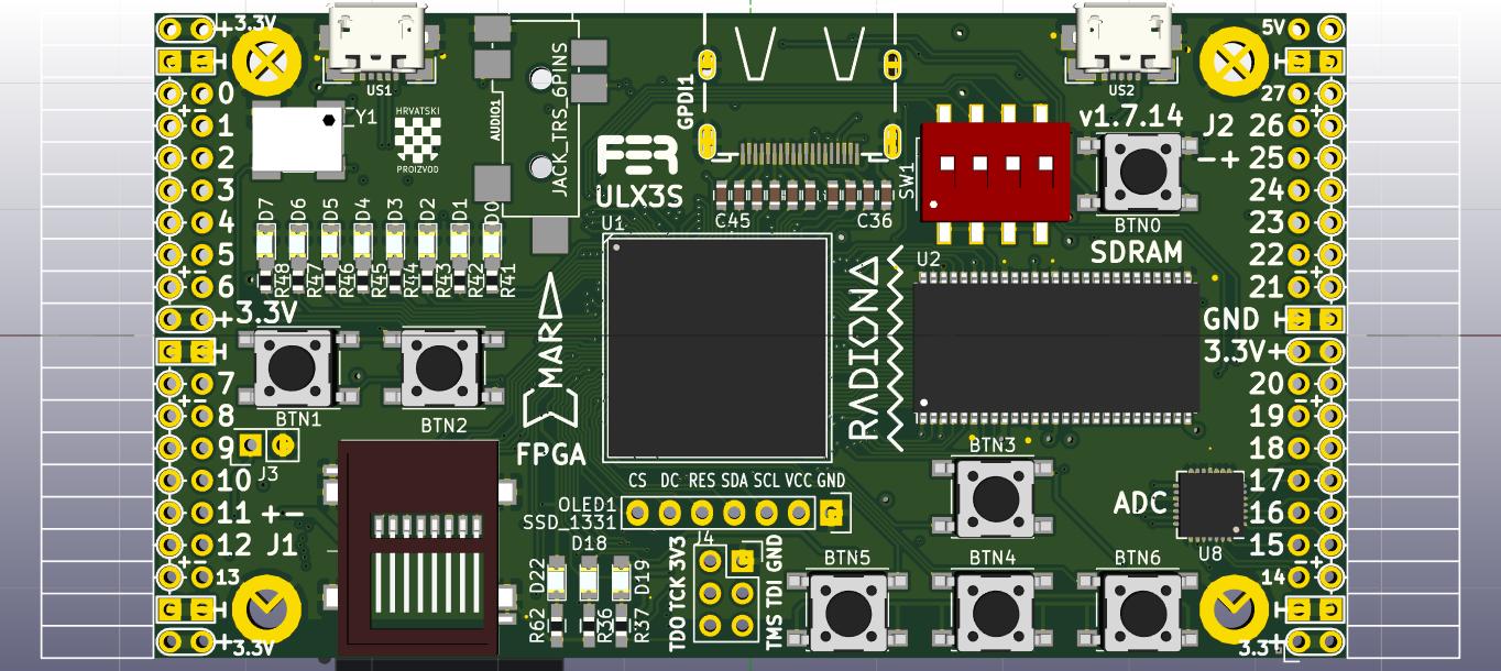
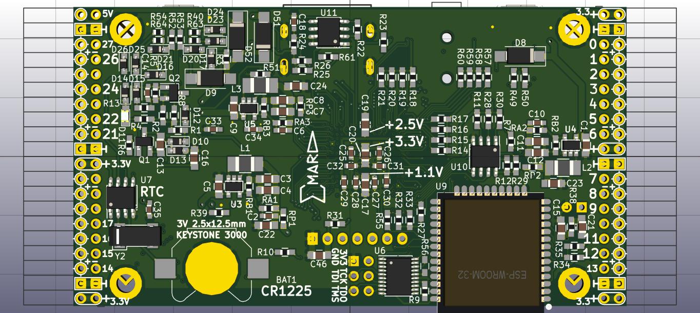
This is a small (94x51 mm) standalone FPGA board for education, research and general purpose, with a full featured selection of chips which I all wanted on a low-cost PCB, but haven't found on the market. It's open source and open hardware because if it is good for our development on f32c SOC, it should be also good to other projects.
ULX3S will carry all digital logic on our research, education and makerspace projects in next 5 years.
ULX3S is standalone embeddable gadget with onboard display, buttons, storage, WiFi and compatible connectors.
ULX3S can do things no other board can.
ULX3S can self-reflash with a bitstream sent remotely from web interface over WiFi or from SD card browsed by onboard OLED display and buttons.
ULX3S can completely power down and wakeup from battery backed RTC.
ULX3S has rich range of chips and connectivity required for many other open source projects: SDRAM, USB, PS/2, SDCARD, HDMI, FLASH, RTC, I2C, OLED, AUDIO, ADC, onboard FM/ASK antenna 88-433.92 MHz and 56 GPIO pins which are all routed as differential pairs and have pinout that is PMOD compatible.
ULX3S is sufficiently equipped to emulate Amiga retro computer and run its games, but can do much more.
Schematics and PCB are done in open source KiCAD PCB editor:
kicad ulx3s.pro
PCB v1.7 is produced. Important board features are tested and work like USB-JTAG, SDRAM, SDCARD, HDMI, FLASH, RTC, I2C, OLED, AUDIO, ADC, 433.92MHz US2 can be used to plug USB-PS/2 combo keyboard but US2 feature as USB host/device is not tested. There are known issues, luckily most can be fixed by Upgrading PCB v1.7.
Features
FPGA: Lattice ECP5 LFE5U-45F-6BG381C
USB: FTDI FT231XS (300kbit JTAG and 3Mbit USB-serial)
GPIO: 56 pins (28 differential pairs), PMOD-friendly
RAM: 32MB SDRAM MT48LC16M16
Flash: 4MB SPI Flash IS25LP032D for FPGA config
Storage: Micro-SD slot
LEDs: 11 (8 blink-LEDs, 2 USB LEDs, 1 WiFi LED)
Buttons: 7 (4 direction, 2 fire, 1 power button)
Audio: 3.5 mm jack with 4 contacts (analog stereo + digital audio or composite video)
Video: GPDI connector with 3.3V-5V I2C bidirectional level shifter
Display: placeholder for 0.96" SPI COLOR OLED
WiFi+bluetooth: placeholder for ESP-32 (Standalone JTAG web interface over WiFi)
ADC: 8 channels, 8 bit, 1 MSa/s MAX11123
Power: 3 Switching voltage regulators: 1.1V, 2.5V, 3.3V
Clock: 25 MHz onboard, external differential clock input
Low power sleep: RTC clock wakeup, power button, 32768 Hz quartz and battery
GPDI is General Purpose Differential Interface, Electrically LVDS, mostly TMDS tolerant female receptacle more-or-less compatible with digital monitors/TVs
Todo
Test the prototype.
[x] Silkscreen Double outline for BGA chip
[x] Silkscreen do not write over the solder pads
[x] Silkscreen JTAG signal names on 6-pin 2.54 mm header
[x] Silkscreen remove OLED outline
[x] Solder stop mask must go inbetween all SMD chip pads
[x] External differential clock input at J1_33 +/-
[x] physically sprinkle VCC blocator capacitors under BGA
[ ] Values on silkscreen
[x] Dedicated antenna pin
[x] onboard 433 antenna
[x] 433 remove GND and silkscreen test point
[x] Resistors for LEDs
[x] Move USB LEDs from bottom to top side
[x] Improve SDRAM routing - use VIAs for closest pins
[x] Increase thickness of power lines (5V, 3.3V, 2.5V)
[x] Compile a f32c bitstream using the schematics
[x] Compile differential GPDI output
[x] Connect more lines from ESP-32 to FPGA
[x] Connect FPGA USB D+/D- with 1.5k pullup in USB 1.1 (full speed) mode
[x] FPGA USB add 27 ohm + 3.6 V zener
[x] Symmetrically place USB connectors left-right
[ ] Jumpers to switch 2.5V/3.3V for left IO banks
[x] External JTAG header
[x] Move JTAG 2 mm left
[x] Move WiFi Disable jumper closer to the BTN1 (angled header)
[x] Sprinkle 2.2uF capacitors on power lines
[x] Spice simulation of power-up/shutdown network
[x] 27ohm D+/D- to FT231XS
[x] DIP switch (4 switches)
[x] MAX11123 ADC SPI
[x] I2C for RTC
[x] main usb connector on top side
[x] space screw to other parts
[x] move battery away from screw hole
[x] top layer GND fill
[x] R25 move away from oled screw hole
[x] DIP switch to the right near RAM
[x] Move HDMI a bit closer to OLED
[x] 32768Hz oscillator footprint
[x] SD card footprint SCHD3A0100
[x] center the SD footprint for T&R
[x] SD connect GND (thin pins)
[x] move USB 0.5-1mm more out
[x] DIP SW footprint correct
[x] AUDIO jack footprint fits
[x] AUDIO jack pin 4 (ring2) connected to 4-bit DAC
[x] BTN footprint too small
[x] SMPS jumpers default OFF for prototype testing
[x] FPGA DONE to ESP-32
[x] Diodes manual soldering
[x] R56: FT231X rev A,B,C TXDEN to GND
    workaround from TN140_FT231X Errata
[x] PCB for LFE5UM ready (some GND will change to
    VCC for Serdes power supply, see LFE5U->LFE5UM
    migration docs)
[x] Check GND/VCC for 45 and 85 packages,
    for example pin T11 is NC on 25U, GND on 85U and VCC ond 85UM
[x] Reconnect WIFI_OFF so that jumper has priority
[x] 25MHz oscillator: needs clearance from LEDs, move under USB1
[x] connect SHUTDOWN to FPGA
[ ] ESP-32: GPIO12 at boot selects internal flash voltage,
    it is connected to J1_27+ and wrong pullup/pulldown at boot
    will prevent ESP32 from booting
[x] ESP-32: won't boot when SD connected. Don't solder it at PCB v1.7
    It is routed differently in newer release
    Arduino->Examples->ESP32->SD_MMC_Test
    https://github.com/espressif/esp-idf/blob/master/examples/storage/sd_card/README.md
    moved blue LED from GPIO2 to GPIO5
[x] I2C resistors increased 470->2.2k
[x] GPDI AC-coupling 100nF to each differential line.
[x] reliable shutdown (D11=RED LED, R4=4.7k)
[x] SDRAM raster back to 0.8 mm
[x] connect SPI Flash Quad Mode (QSPI)
[x] allow powering the board without powering FTDI chip
[ ] reverse D9 at US2 to draw power from usb instead of provide it
[x] micro USB extended pads for Handsoldering (already were extended)
[x] move 25MHz oscillator away from USB connector for handsoldering
[x] schematics gpio J..+- pins renamed to gp/gn for easier readability
[ ] Make BOM outputtable from PCB->Files->Fabrication Outputs->BOM file
[ ] route 16-channel ADC
[x] move 8 LEDs a bit down and right
[x] let SD_CLK go to FPGA clock capable pin: swap SD_CLK and SD_D2 pins
[x] additional 2 differential lines for US2
[x] additional US2 pins for pullup 1.5k
[x] additional US2 pins for pull up-down 15k
[x] unified US2 pullup/down: resistor-diode nework for pullup 1.5k and pulldown 15k
[x] clear silkscreen mess with Cx under FPGA
[x] power decoupling capacitors for ESP32 and OLED
[x] Connect switching power supply jumpers
[ ] every 1-2 seconds there are clicks at analog audio output
[x] 3.6V zener diodes must be on FPGA side