|
|
8 years ago | |
|---|---|---|
| doc | 8 years ago | |
| footprints | 8 years ago | |
| pic | 8 years ago | |
| plot | 8 years ago | |
| spice | 9 years ago | |
| tools | 9 years ago | |
| .gitignore | 9 years ago | |
| README.md | 8 years ago | |
| analog.bak | 8 years ago | |
| analog.sch | 8 years ago | |
| blinkey.bak | 8 years ago | |
| blinkey.sch | 8 years ago | |
| flash.bak | 8 years ago | |
| flash.sch | 8 years ago | |
| fp-lib-table | 9 years ago | |
| gpdi.bak | 8 years ago | |
| gpdi.sch | 8 years ago | |
| gpio.bak | 8 years ago | |
| gpio.sch | 8 years ago | |
| power.bak | 8 years ago | |
| power.sch | 8 years ago | |
| ram.bak | 8 years ago | |
| ram.sch | 8 years ago | |
| sdcard.bak | 8 years ago | |
| sdcard.sch | 8 years ago | |
| ulx3s-cache.lib | 8 years ago | |
| ulx3s-rescue.lib | 9 years ago | |
| ulx3s.bak | 8 years ago | |
| ulx3s.kicad_pcb | 8 years ago | |
| ulx3s.kicad_pcb-bak | 8 years ago | |
| ulx3s.pro | 8 years ago | |
| ulx3s.sch | 8 years ago | |
| usb.bak | 8 years ago | |
| usb.sch | 8 years ago | |
| wifi.bak | 8 years ago | |
| wifi.sch | 8 years ago | |
README.md
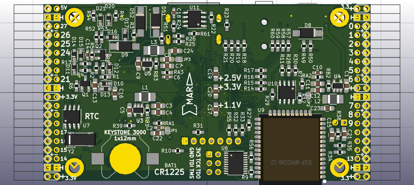
ULX3S PCB
This is work-in-progress place for putting some wishes of a small (94x51 mm) FPGA board.
ULX3S = University digital logic Learning eXtensible board release 3 with SDRAM, Successor of ULX2S.
kicad ulx3s.pro
Schematics is mostly complete. PCB routing is mostly complete too. PCB produced when at version 1.7 and big things work like USB-JTAG, SDRAM, SDCARD, HDMI, FLASH, RTC, I2C but there are issues: PCB v1.7 has small issues like SHUTDOWN not connected. When SHUTDOWN is released, usually board wakes up again, cause of that is unknown, could be RTC waking it up. WIFI won't work if its pins to SDCARD are connected, WIFI disable jumper won't work if wifi enable is held high by FPGA. For some monitors I2C works and for some it doesn't. Maybe 470 resistors should be increased to 1.2k. AUDIO, OLED are currently untested.
3D preview
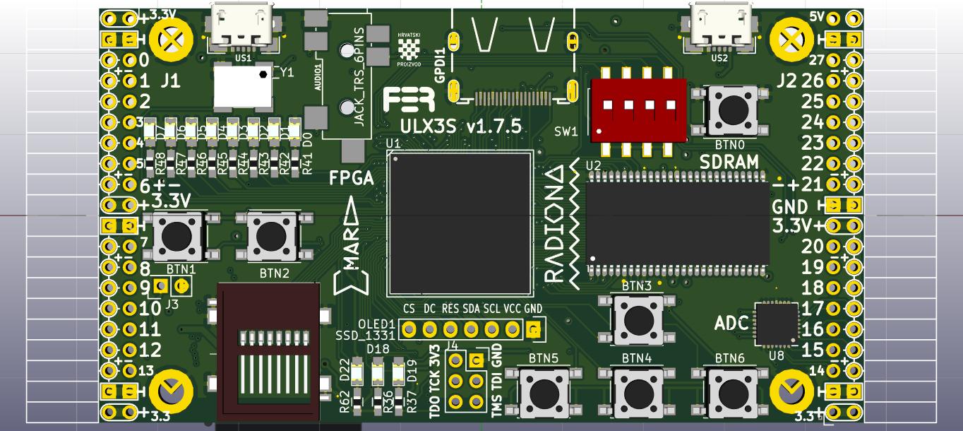
Features
FPGA: Lattice ECP5 LFE5U-45F-6BG381C
USB: FTDI FT231XS (300kbit JTAG and 3Mbit USB-serial)
GPIO: 56 pins (28 differential pairs), PMOD-friendly
RAM: 32MB SDRAM MT48LC16M16
Flash: 4MB SPI Flash IS25LP032D for FPGA config
Storage: Micro-SD slot
LEDs: 11 (8 blink-LEDs, 2 USB LEDs, 1 WiFi LED)
Buttons: 7 (4 direction, 2 fire, 1 power button)
Audio: 3.5 mm jack with 4 contacts (analog stereo + digital audio or composite video)
Video: GPDI connector with 3.3V-5V I2C bidirectional level shifter
Display: placeholder for 0.96" SPI COLOR OLED
WiFi+bluetooth: placeholder for ESP-32 (JTAG and serial over WiFi)
ADC: 8 channels, 12 bit, 1 MSa/s MAX11123
Power: 3 Switching voltage regulators: 1.1V, 2.5V, 3.3V
Clock: 25 MHz onboard, external differential clock input
Low power sleep: RTC clock wakeup, power button, 32768 Hz quartz and battery
GPDI is General Purpose Differential Interface, Electrically LVDS, mostly TMDS tolerant female receptacle more-or-less compatible with digital monitors/TVs
Todo
Make the prototype.
[x] Silkscreen Double outline for BGA chip
[x] Silkscreen do not write over the solder pads
[ ] Silkscreen BGA names on ESP32 placeholder and 2.54 mm headers
[x] Silkscreen JTAG signal names on 6-pin 2.54 mm header
[x] Silkscreen remove OLED outline
[x] Solder stop mask must go inbetween all SMD chip pads
[x] External differential clock input at J1_33 +/-
[ ] Thinner copper, more spacing to SDRAM-FPGA
[x] physically sprinkle VCC blocator capacitors under BGA
[ ] Values on silkscreen
[x] Dedicated antenna pin
[x] onboard 433 antenna
[x] 433 remove GND and silkscreen test point
[x] Resistors for LEDs
[x] Move USB LEDs from bottom to top side
[x] Improve SDRAM routing - use VIAs for closest pins
[x] Increase thickness of power lines (5V, 3.3V, 2.5V)
[x] Compile a f32c bitstream using the schematics
[x] Compile differential GPDI output
[x] Connect more lines from ESP-32 to FPGA
[x] Connect FPGA USB D+/D- with 1.5k pullup in USB 1.1 (full speed) mode
[x] FPGA USB add 27 ohm + 3.6 V zener
[x] Symmetrically place USB connectors left-right
[ ] Jumpers to switch 2.5V/3.3V for left IO banks
[x] External JTAG header
[x] Move JTAG 2 mm left
[x] Move WiFi Disable jumper closer to the BTN1 (angled header)
[x] Sprinkle 2.2uF capacitors on power lines
[x] Spice simulation of power-up/shutdown network
[x] 27ohm D+/D- to FT231XS
[x] DIP switch (4 switches)
[x] MAX11123 ADC SPI
[x] I2C for RTC
[x] main usb connector on top side
[ ] space screw to other parts
[x] move battery away from screw hole
[x] top layer GND fill
[x] R25 move away from oled screw hole
[ ] board cut off notches inisde for space saving
[x] DIP switch to the right near RAM
[x] Move HDMI a bit closer to OLED
[x] 32768Hz oscillator footprint
[x] SD card footprint SCHD3A0100
[x] center the SD footprint for T&R
[x] SD connect GND (thin pins)
[x] move USB 0.5-1mm more out
[x] DIP SW footprint correct
[x] AUDIO jack footprint fits
[x] AUDIO jack pin 4 (ring2) connected to 4-bit DAC
[x] BTN footprint too small
[x] SMPS jumpers default OFF for prototype testing
[x] FPGA DONE to ESP-32
[x] Diodes manual soldering
[x] R56: FT231X rev A,B,C TXDEN to GND
    workaround from TN140_FT231X Errata
[x] PCB for LFE5UM ready (some GND will change to
    VCC for Serdes power supply, see LFE5U->LFE5UM
    migration docs)
[x] Check GND/VCC for 45 and 85 packages,
    for example pin T11 is NC on 25U, GND on 85U and VCC ond 85UM
[x] Reconnect WIFI_OFF so that jumper has priority
[x] 25MHz oscillator: needs clearance from LEDs, move under USB1
[ ] connect SPI Flash Quad Mode (QSPI)
[x] connect SHUTDOWN to FPGA
[ ] ESP-32: GPIO12 at boot selects internal flash voltage,
    it is connected to J1_27+ and wrong pullup/pulldown at boot
    will prevent ESP32 from booting
[ ] ESP-32: won't boot when SD connected. Don't solder it at PCB v1.7
    it should be routed differently in newer release
[x] I2C resistors increased 470->2.2k
[ ] GPDI series C=100nF to each differential line.