3.8 KiB
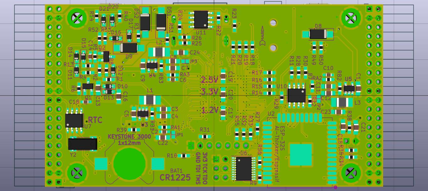
ULX3S PCB
This is work-in-progress place for putting some wishes of a small (94x51 mm) FPGA board.
ULX3S = University digital logic Learning eXtensible board release 3 with SDRAM, Successor of ULX2S.
kicad ulx3s.pro
Schematics is mostly complete. PCB routing is mostly complete too.
3D preview
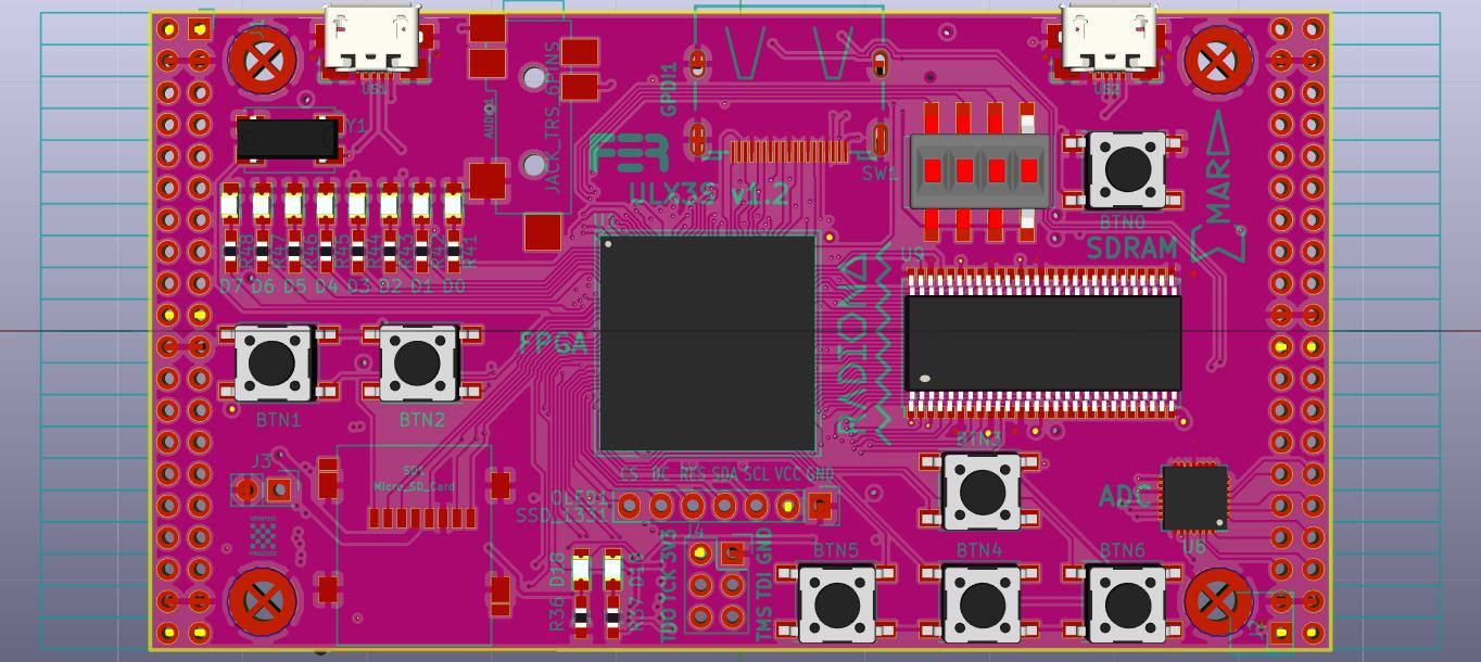
Features
FPGA: Lattice ECP5 LFE5U-25F-6BG381C
USB: FTDI FT231XS (1Mbit JTAG and 3Mbit usbserial)
GPIO: All differential, PMOD-friendly
RAM: 32MB SDRAM MT48LC16M16
Flash: 8MB SPI flash S25FL164 for FPGA config
Storage: Micro-SD slot
LEDs: 10 (8 blink-LEDs, 2 USB leds)
Buttons: 7 (4 direction, 2 fire, 1 power button)
Audio: 3.5 mm stereo jack
Video: GPDI connector with 3.3V-5V I2C bidirectional level shifter
Display: placeholder for 0.96-1.3" SPI OLED COLOR or B/W
WiFi+bluetooth: placeholder for ESP-32 (JTAG and serial over WiFi possible)
ADC: 8 channels, 12 bit, 1 MSa/s MAX11123
Power: 3 Switching voltage regulators: 1.2V, 2.5V, 3.3V
Clock: 25 MHz onboard, external differential clock input
Low power sleep: RTC clock wakeup, power button, 32768 Hz quartz and battery
GPDI is General Purpose Differential Interface, Electrically LVDS, mostly TMDS tolerant female receptacle more-or-less compatible with digital monitors/TVs
Todo
Make the prototype.
[x] Silkscreen Double outline for BGA chip
[x] Silkscreen do not write over the solder pads
[ ] Silkscreen BGA names on ESP32 placeholder and 2.54 mm headers
[x] Silkscreen JTAG signal names on 6-pin 2.54 mm header
[x] Silkscreen remove OLED outline
[x] Solder stop mask must go inbetween all SMD chip pads
[x] External differential clock input at J1_33 +/-
[ ] Thinner copper, more spacing to SDRAM-FPGA
[x] physically sprinkle VCC blocator capacitors under BGA
[ ] Values on silkscreen
[x] Dedicated antenna pin
[x] onboard 433 antenna
[ ] 433 remove GND and silkscreen test point
[x] Resistors for LEDs
[x] Move USB LEDs from bottom to top side
[ ] Improve SDRAM routing - use VIAs for closest pins
[x] Increase thickness of power lines (5V, 3.3V, 2.5V)
[x] Compile a f32c bitstream using the schematics
[x] Compile differential GPDI output
[x] Connect more lines from ESP-32 to FPGA
[x] Connect FPGA USB D+/D- with 1.5k pullup in USB 1.1 (full speed) mode
[x] FPGA USB add 27 ohm + 3.6 V zener
[x] Symmetrically place USB connectors left-right
[ ] Jumpers to switch 2.5V/3.3V for left IO banks
[x] External JTAG header
[x] Move JTAG 2 mm left
[ ] Move WiFi Disable jumper above the buttons
[x] Sprinkle 2.2uF capacitors on power lines
[x] Spice simulation of power-up/shutdown network
[x] 27ohm D+/D- to FT231XS
[x] DIP switch (4 switches)
[x] MAX11123 ADC SPI
[x] I2C for RTC
[x] main usb connector on top side
[ ] space screw to other parts
[x] move battery away from screw hole
[x] top layer GND fill
[x] R25 move away from oled screw hole
[ ] board cut off nothches inisde for space saving
[x] DIP switch to the right near RAM
[x] Move HDMI a bit closer to OLED
[x] 32768Hz oscillator footprint
[x] SD card footprint SCHD3A0100
[ ] SD use CD (card detect) contacts
[x] move USB 0.5-1mm more out
[x] DIP SW footprint correct
[x] AUDIO jack footprint fits
[ ] AUDIO jack pin 4 not connected
[x] BTN footprint too small
[x] SMPS jumpers default OFF for prototype testing
[x] FPGA DONE to ESP-32
[x] Diodes manual soldering
[x] R56: FT231X rev A,B,C TXDEN to GND
    workaround from TN140_FT231X Errata
[ ] PCB for LFE5UM ready (some GND will change to
    vcc for Serdes power supply, see LFE5U->LFE5UM
    migration docs)
[ ] Check GND/VCC for 45 and 85 packages,
    for example pin T11 is NC on 25U, GND on 85U and VCC ond 85UM